How to Design a PCB Layout Circuit Diagram
How to Design a PCB Layout Circuit Diagram PCB layout design is the process of arranging electronic components, conductive traces, power planes, and other elements on a circuit board to facilitate the flow of electrical signals and meet the functional requirements of the electronic system. Connect all ground points to the ground plane to create a low impedance return path for
Create Gerber Files in KiCad. From the PCB Editor in KiCad you can create Gerber files by going to the File menu and selecting Plot… A window will appear. Click on the Plot button to create the Gerber files. To create Drill files, click on Generate Drill Files… to open the Drill File dialog. Then click the button Generate Drill File. Step 3: PCB layout stage. The PCB layout stage includes setting up the design tool, board outline, netlist import, component placement, routing, silkscreen cleanup, DRC check, and generating documents for production (Gerbers, netlist, etc.). Setting up the stack-up. The board layout is started by setting the stack-up and design rules.
How to Design a PCB Layout? Circuit Diagram
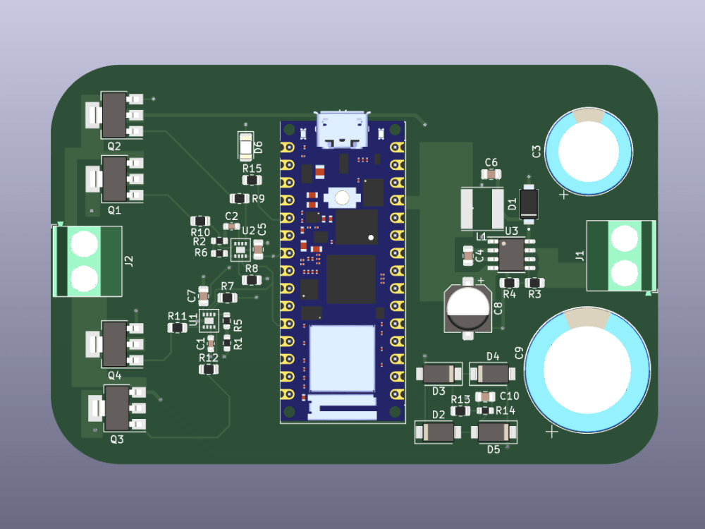
Step 3: Create PCB layout. Convert schematics into PCB layouts. Select the appropriate PCB size and shape, which takes into account space for mounting, heat dissipation requirements, and fit with other PCBs. Components are shown as footprints with pads and connection lines in the PCB layout. You can see how the components will physically look

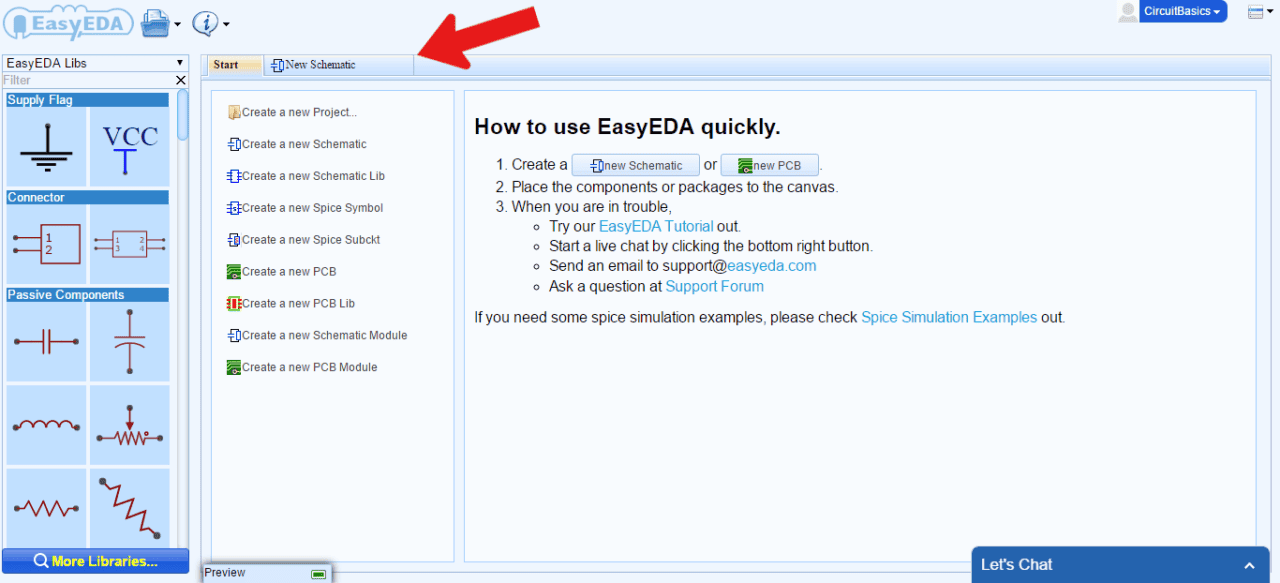
For beginners, TechSparks recommends initiating the design process with the PCB schematic.The schematic serves as the foundation for circuit design, illustrating the interconnection relationships among electronic components and circuit functions. Guided by the schematic, the designer strategically plans and arranges the placement of electronic components on the PCB.

How to DIY design PCB layout by yourself Circuit Diagram
Step 4: Get Your PCB Made. When you're finished drawing your PCB design, you need to get the design made. You could etch your PCB at home, but my preferred way is to just order a PCB from one of the many PCB manufacturers out there.
